
Applications

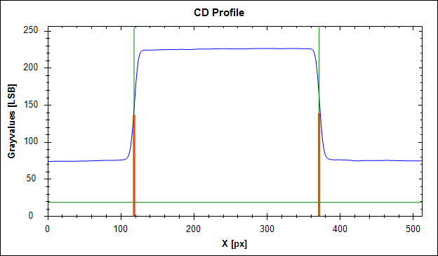
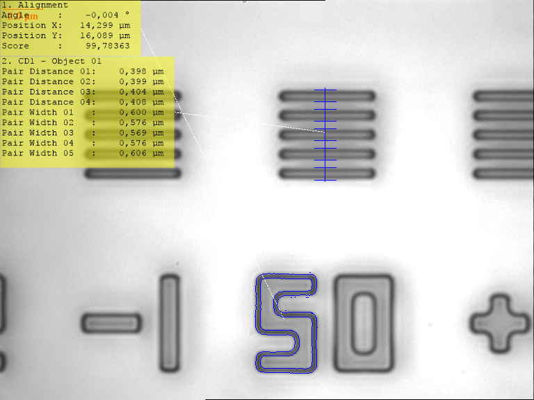
CD Measurement
Optical overlay and structure with measurement based on light microscopes is a proven, non-contact and fast measuring method.
The extreme precision of the measurement results is due to powerful algorithms and the perfectly coordinated combination of microscope, camera and software.
Programmed measuring positions are approached exactly, new measuring coordinates can be learned quickly through teaching or import. The programmed measurement structures are positioned precisely using image alignment. A high-resolution digital CCD camera records images whose gray value intensity profiles are used for the subpixel algorithms.
The laser autofocus ensures operator-independent, reproducible focusing.
Further measurement options with this application include:
- Measurement of edge stripping on bare wafers

Overlay Measurement
Optical overlay and CD measurement based on light microscopes has proven itself as a non-contact and fast measuring method.
The extreme precision of the measurement results is due to powerful algorithms and the perfectly coordinated combination of microscope, camera and software.
Programmed measuring positions are approached exactly, new measuring coordinates can be learned quickly through teaching or import.
With our MCS system software, a combination of different tasks such as CD and thin film thickness measurement or automatic inspection in a mixed process is possible.
Defect review
In our MCS software we use a universally adjustable optical defect review.
We offer our optical review with defect classification, based on imported data from a defect scanning system (e.g. KLARF files). We use various sorting options and can display the defects on a zoomable overview map.
Precise and fast positioning of the selected defects is possible, even at the highest magnification.
With our automatic review, images of the defect with several contrast methods can be taken and saved.
In combination with a refurbished INS3000 we can offer you a complete makro- and micro-inspection and review tool.


Thin-film Measurements
With the reflectometry, we can measure thin-film measurements on our microscopes.
Typically, layer thicknesses from a few nanometers to micrometers can be measured. Depending on the task, different spectrometers and light sources are used. The Nanocalc software is used to evaluate and qualify the measurement signal. Our MCS software controls the measurement and collects the data to transfer it into appropriate output files.
The layer thickness measurement is integrated into the microscope in such a way that additional functions such as CD measurement or inspection tasks are possible.
Using Deep UV, we are now able to measure thin layers below 10nm, depending on the layer structure. With our high-resolution IR-spectrometers, we are also able to measure thick coatings very precisely.
Depending on the measurement tasks, we can equip our microscopes with one or more spectrometers to measure the desired layer thickness.
A standard feature of our software is the 2D or 3D maps to analyze the measurements.

Golden Template Matching
Golden Template Matching is a high-performance method for finding defects on structured wafers. It is particularly suitable for die-based wafers.
It can detect contamination, breakouts, coating defects and other defects.
For Golden Template Matching, a few reference images are first taken to determine what a perfect die looks like.
This image of a perfect die is then used as a template.
During the scan, the images of the dies are then compared with the template and deviations are output as defects if they exceed the sensitivity parameters you have set.
Deep Learning
Deep learning is now an established way of detecting and classifying process errors, visual defects or other irregularities.
Unlike template matching, a neural network must first be trained by a human.
The training environment we provide enables you to train and combine neural networks in different ways in an intuitive interface to suit your applications.
These can include defect detection, counting structures, classifying structures and/or defects, OCR or a combination of all these possibilities.
We would be happy to discuss your individual application with you.
Bond Ring Inspection
Using IR transmitted light, we can achieve excellent results when measuring bonded wafers. Classic measurements such as CD or overlay measurements are no problem with our IR microscopes. Special software features make it possible to focus the position to be measured very well, which is a requirement for good IR measurements.
Stitching
Stitching involves combining many smaller individual images into one large image.
It is used when a single field of view is no longer enough, e.g. to image a large defect or to document an entire wafer.
A stitched image can be created in our software both manually and in recipes (automatically).
We look forward to a demonstration of the tool with your inquiry.
Customer demonstration
I need a demonstration or further product information.
Price information
I need a price or product configuration.
Application service
I need information, support, or training for the applications on my system.
Customer service
I need technical support, software information or other service.